


Panelization Test - One Panel for testing different PCBs
Why PCB panel testing?
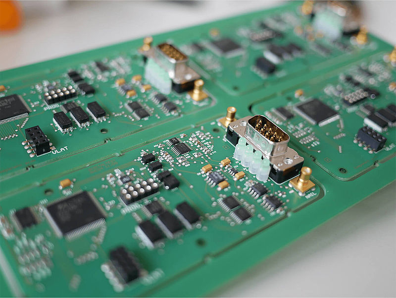
Fitting PCBs in panels (PCB panelization) has become a trend in electronic manufacturing in recent years, because of its power to save on resources. Manufactoring many PCBs in panels saves time and money. However what is it like when it comes to in-circuit or function testing of the finished circuit boards? Many electronics manufacturers are still cautious when it comes to panel testing. The advantages are obvious: even the smallest boards can be tested, the assembly is twist-proof thanks to its dual use, and higher quantities can be tested in a shorter time with less use of resources.
Is there additional effort preparing the data when doing panelization testing?
Panel definitions are more time-consuming and sometimes very complex. Therefore, there is additional effort. However, this can be minimized by suitable software. Our CAD/CAM software C-LINK with its various functions provides assistance for all common test systems. It is possible, for example, to import a panel file from the CAD data of a single board, to define the PCB numbering or to summarize the panel as a single board with a one-click operation. Fixture design also presents the developer with greater challenges than with a single panel. C-LINK facilitates automation: The software independently transfers the pin position, selection of the pin properties, pin numbering and documentation to all PCBs in the panel.
Fast test program creation for panelization tests
Neither the creation nor the debugging require more time with the system software CITE - there is a test program for all single boards. The Digitaltest software also supports mixed panels; only one test program is required for each single board. If a single unit is to be excluded from the test - for example because it is obviously defective or simply does not exist - this can be done automatically via the interface to the upstream process or manually, using a simple graphical selection.
Does panel testing lead to bottlenecks in the production line?
If, for example, the test system is to test an eight-fold panel instead of a single unit, this requires more time within the production line - a jam could occur. Here, a parallel test can reduce the test time to such an extent that the user test fits into the cycle time of the line. With the parallel technology of Digitaltest, the Lambda edition, the single boards are tested simultaneously on the multiple panel and thus the tests are carried out in the fastest way. This works by performing an in-circuit test, or functional test on two or more independent test heads, thereby reducing the test time by the corresponding factor.
Traceability of errors when panel testing
If the modules are very low-priced, the production costs change little if a faulty multi panel is disposed of instead of a single PCB. As soon as it pays to repair the defective module, this poses a challenge during the panel test: Where is the fault located? The paperless repair software QMAN for all common test systems finds the fault. The integrated repair station displays the panel number via the fault import of the panel log file. In addition, the exact fault location on the single board and the defective component are displayed in detail. In this way, the repairer knows exactly which component on which single board is faulty within which panel. Anyone who has now included a test area for field returns in the fixture design can easily test the repaired single PCB again.