


Design Verification
Our Design Verification Service offers
- Clarify test request
- Check the suitability of the data
- Communicate with customers
- Communicate with suppliers
- Create test proposal
- Estimate cost
- Sketch a time schedule
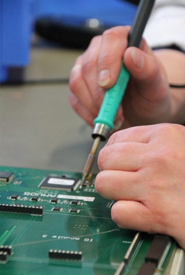
Design for Testability (DFT)
Do you need help with the design for testability (DFT) verification of your pcb? Depending on which test methods you use, we can determine the test coverage. Tell us if you are using analog in-circuit test (ICT), digital ICT, flying probe test, functional test or a combination of these tests. We analyze the design data and calculate the test coverage possible with the available test equipment.
You can determine the depth of the design verification. If, for example, only an assessment of the contactability by means of a bed of nail fixture is desired, fixture specific parameters (such as minimum pad sizes, needle diameter, snap-in positions, vacuum interface or inline with pneumatic press system, etc.) are used in the test. The theoretical testability of the pcb, resulting from the contacting, can be prepared after a further, deeper evaluation a preliminary testcoverage report.
In addition to the above-mentioned evaluations, an estimation for the test time can be given for Digitaltest systems (ICT and Flying-Probe). This is an important piece of information for process planning. If the number of pieces is high, the possible cycle time can be recognized at an early stage and the best strategy, such as test balancing or parallelization (Lambda edition), can be selected.